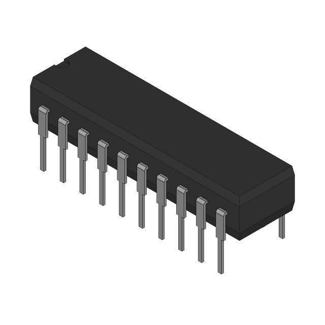
The Texas Instruments CDC208N is a high-performance clock distribution and buffer integrated circuit designed to provide low-skew, low-jitter clock fan-out for digital systems requiring precise timing alignment across multiple synchronous subsystems. It is part of TI’s CDC (Clock Driver/Clock Distribution) family, which is optimized for distributing a single reference clock to multiple outputs with controlled propagation delay, matched output timing, and minimal additive phase noise. The device is primarily used in systems where deterministic clock phase alignment is required across multiple loads such as high-speed digital logic, communication subsystems, and mixed-signal processing platforms.
## Device Function and Electrical Positioning
The CDC208N functions as a clock buffer and fan-out distribution device, receiving a single or differential clock input and generating multiple buffered output clock signals. Its primary role is to maintain signal integrity and timing consistency while driving multiple loads that would otherwise degrade the quality of the reference clock source.
The device is designed to operate in synchronous digital environments where clock skew and jitter directly affect system timing margins. It ensures that all output channels maintain tight propagation delay matching relative to the input reference clock, enabling reliable multi-load synchronization in high-speed digital architectures.
Unlike simple logic buffers, the CDC208N is optimized for low additive jitter and controlled output transition characteristics, which are critical for maintaining timing accuracy in high-frequency clock networks.
## Internal Architecture and Signal Path Design
The CDC208N is implemented using a high-speed CMOS clock buffer architecture with internal signal conditioning stages. The input stage conditions the incoming clock signal to ensure proper logic-level detection and noise immunity. This is followed by a distribution network that routes the signal to multiple output driver stages.
Each output stage is independently buffered to provide consistent drive strength and controlled edge rates. The internal architecture is designed to minimize channel-to-channel skew by carefully matching propagation paths and balancing internal load capacitances.
The device uses symmetrical layout techniques to ensure that each output experiences nearly identical electrical delay characteristics. This is essential for applications requiring phase alignment across multiple clock domains.
## Electrical Characteristics and Defined Parameters
The electrical parameters of the CDC208N are defined in terms of timing performance, logic-level compatibility, and output drive capability. These parameters are specified under controlled operating conditions in the datasheet and are critical for system-level timing analysis.
Supply voltage (VCC): Defines the operating voltage range of the internal CMOS logic and output driver stages. This parameter determines compatibility with standard TTL/CMOS logic families.
Input clock frequency range: Specifies the allowable frequency range of the input reference clock. The device is designed to operate within a defined frequency band suitable for digital system clock distribution.
Propagation delay (tPD): Represents the time delay between the input clock edge and corresponding output clock edge. This parameter is critical for determining clock latency in synchronous systems.
Output-to-output skew: Defines the maximum timing difference between any two output channels under identical loading conditions. This parameter is essential for multi-load synchronization accuracy.
Rise and fall times (tR, tF): Characterize the output signal edge transition speed, which affects signal integrity, electromagnetic interference, and timing margin.
Output drive capability: Specifies the maximum capacitive load each output can drive while maintaining defined timing and voltage levels. This parameter is critical for PCB clock tree design.
Additive jitter: Represents the additional timing uncertainty introduced by the device to the input clock signal. Low additive jitter is a key requirement for high-performance clock distribution.
Duty cycle distortion: Defines the deviation of output duty cycle from an ideal 50 percent, which can affect timing symmetry in clocked systems.
## Logic Interface and Signal Integrity Behavior
The CDC208N is designed for compatibility with standard CMOS and TTL logic levels depending on supply configuration. The input stage is designed to provide high noise immunity, ensuring reliable operation in electrically noisy environments typical of high-speed digital systems.
The output drivers are designed to maintain fast, controlled edge rates while minimizing overshoot and undershoot. Controlled edge shaping reduces high-frequency spectral content, thereby improving electromagnetic compatibility performance in densely packed digital systems.
Signal integrity is preserved through careful internal impedance control and output stage symmetry. This ensures minimal reflection and consistent waveform shape across all output channels, even under varying load conditions.
## Clock Distribution Performance Characteristics
A key functional requirement of the CDC208N is maintaining deterministic timing relationships between multiple output clocks. This is achieved through internal matching of propagation delay paths and uniform output buffer design.
Skew performance is a primary specification, as even small timing differences between clock outputs can introduce setup and hold violations in synchronous digital systems. The device is optimized to minimize both static skew (device-to-device variation) and dynamic skew (load-dependent variation).
Jitter performance is equally critical, as added timing uncertainty directly impacts system timing margins. The CDC208N is designed to introduce minimal phase noise, preserving the spectral purity of the input reference clock.
## Package and Mechanical Characteristics
The CDC208N is typically provided in a dual in-line package (DIP) format, consistent with legacy digital logic IC packaging. The package is designed for through-hole PCB mounting, providing mechanical robustness and ease of integration in prototyping and industrial environments.
The internal lead frame structure is optimized for low inductance signal paths, which is important for maintaining clean clock edges at high switching speeds. The package also provides sufficient pin spacing for standard PCB design rules in mixed-signal digital systems.
Thermal performance is not a primary limiting factor for this device due to its relatively low power dissipation in clock buffering applications. However, proper PCB layout is still required to ensure stable operation and noise immunity.
## System-Level Design Considerations
Proper power supply decoupling is essential for maintaining low jitter performance. Local bypass capacitors must be placed close to the supply pins to minimize supply noise coupling into the internal clock distribution network.
PCB layout symmetry is important to preserve output-to-output skew performance. Unequal trace lengths or loading conditions can degrade timing alignment across output channels.
Termination strategies may be required depending on trace length and system frequency. Proper impedance matching helps prevent reflections that can distort clock edges and introduce timing uncertainty.
The CDC208N is typically used in conjunction with a stable reference oscillator or PLL-based clock generation system, forming part of a larger hierarchical clock tree architecture.
## Application Domains
The CDC208N is used in synchronous digital systems requiring multiple synchronized clock domains. Typical applications include microprocessor-based systems, digital signal processing platforms, communication equipment, and industrial control systems.
It is also used in test and measurement equipment where precise timing distribution is required across multiple functional modules. Additional applications include data acquisition systems and legacy computing architectures requiring reliable multi-load clock distribution.
The device is particularly suitable for systems where a single master clock must be distributed to multiple subsystems without degradation of timing integrity.
## Conclusion
The Texas Instruments CDC208N is a multi-output clock buffer and distribution device designed to provide low-skew, low-jitter fan-out of a reference clock signal in synchronous digital systems. Its architecture ensures tightly matched propagation delays across multiple outputs, with controlled signal integrity and minimal timing distortion. The device is optimized for deterministic clock distribution in multi-load environments, where timing precision, low additive jitter, and output-to-output skew minimization are critical system-level requirements.