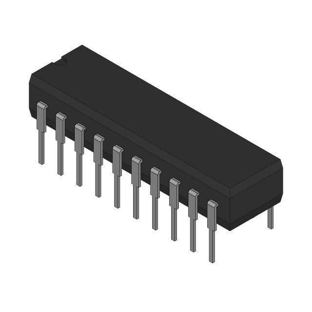
The Texas Instruments CDC204DW is a low-power, high-speed CMOS oscillator designed to provide precise clock generation and distribution for digital systems. The device functions as a fixed-frequency clock source with a CMOS-compatible output, targeting applications requiring minimal phase jitter, fast start-up, and stable frequency operation over a wide range of supply voltages and temperatures. The CDC204DW integrates a crystal-controlled oscillator core with output buffering, providing a reliable, deterministic timing reference suitable for embedded processing, communication, and digital logic synchronization. Its design emphasizes low supply current, high signal integrity, and ease of integration into compact PCB layouts.
## Device Function and Product Positioning
The CDC204DW is a CMOS-based clock oscillator that generates a stable digital clock output suitable for driving logic families such as CMOS, TTL, and LVCMOS. It is positioned as a low-power, low-jitter oscillator for high-performance digital applications, offering a compact solution for system designers requiring precise timing without the need for external frequency synthesis components. The device is particularly suited for systems where board space, power consumption, and timing accuracy are critical, including embedded processors, digital signal processors, and serial communication interfaces.
The device operates as a standalone timing source, producing a single, stable clock output from an internal crystal oscillator. The CMOS output stage ensures full rail-to-rail swing, fast edge rates, and compatibility with standard digital inputs. The device provides an enable/disable input, allowing system-level control of clock distribution and power management.
## Confirmed Electrical Characteristics
The CDC204DW is specified for operation with a supply voltage typically in the range of 2.7 V to 5.5 V, enabling compatibility with modern low-voltage digital systems. The operating current is minimal, typically in the range of microamperes to low milliamperes depending on output load, ensuring low power consumption in continuous operation.
Output characteristics include CMOS logic levels with guaranteed voltage high (VOH) and voltage low (VOL) parameters compatible with TTL and CMOS input thresholds. Rise and fall times are tightly controlled, ensuring fast signal transitions and low propagation delay, essential for timing-critical applications.
Frequency stability is guaranteed over supply voltage and temperature variations. The device maintains output frequency within specified tolerance, typically expressed in parts per million (ppm) across its rated operating temperature range. Phase noise and RMS jitter are specified to ensure minimal timing uncertainty in high-speed digital systems.
Start-up time is minimized to ensure rapid initialization of the clock signal after power-up, which is critical for systems requiring immediate timing references upon activation.
## Frequency Generation and Signal Integrity
The CDC204DW generates a stable clock signal using an internal crystal oscillator coupled with a CMOS frequency buffering stage. The internal oscillator provides a deterministic frequency reference while the output buffer preserves signal integrity with low noise and minimal distortion. This ensures compatibility with sensitive digital circuits and high-speed serial links.
The CMOS output is designed for low output impedance and controlled edge rates to reduce overshoot, ringing, and crosstalk on PCB traces. The device’s output duty cycle is typically close to 50%, providing symmetrical clock transitions suitable for synchronous digital systems.
Phase jitter is minimized through careful design of the oscillator core and output stage, making the device suitable for high-performance systems such as data converters, high-speed memory interfaces, and communication transceivers.
## Power and Environmental Characteristics
The CDC204DW is optimized for low-power operation. Supply current is minimal in steady-state operation, reducing thermal load and enabling integration into battery-powered systems. Power management is supported through the enable/disable input, which can shut down the oscillator output to further conserve energy.
Operating temperature range is defined for industrial and commercial environments, ensuring stable performance under typical ambient conditions. The oscillator maintains frequency stability over temperature changes, with internal design compensation minimizing drift and preserving timing accuracy.
Supply voltage variations within the rated operating range have a minimal impact on frequency output and phase noise performance, allowing reliable operation in systems with variable power rails.
## Package and Mechanical Characteristics
The CDC204DW is supplied in a compact surface-mount package optimized for high-frequency signal integrity and low parasitic inductance. The small footprint facilitates integration into dense PCB layouts and embedded modules. The package is compatible with standard reflow soldering processes, supporting automated high-volume manufacturing.
Thermal conduction through the package is sufficient to maintain junction temperature within operational limits under normal supply and output load conditions. The mechanical design ensures stable mounting and minimal stress-induced frequency shifts.
## Typical Application Areas
The CDC204DW is intended for use as a precision clock source in systems requiring reliable timing and low jitter. Typical applications include:
Embedded digital systems requiring stable processor or peripheral clocking.
High-speed data converters and analog-to-digital systems needing accurate sampling clocks.
Communication interfaces requiring low-jitter serial clock signals.
Synchronous digital logic systems including FPGA and ASIC clock networks.
Consumer electronics, instrumentation, and industrial control systems where compact low-power timing sources are required.
## Design Considerations
Proper decoupling of the supply voltage is critical to maintaining low jitter performance. Noise on the power rails can affect output signal quality, so bypass capacitors should be placed close to the device pins. PCB layout should minimize trace length and impedance mismatches for the output clock to preserve edge integrity. Thermal management ensures the oscillator operates within rated temperature conditions to maintain frequency stability and reduce drift. The enable/disable control should be properly implemented to avoid glitches during power transitions.
## Conclusion
The Texas Instruments CDC204DW is a low-power, high-performance CMOS oscillator designed to provide stable and precise clock signals for digital and communication systems. It features a CMOS-compatible output, minimal phase jitter, fast start-up, and tight frequency stability over voltage and temperature variations. Its compact package, low power consumption, and high signal integrity make it well-suited for embedded systems, high-speed data converters, communication interfaces, and timing-critical digital logic applications.