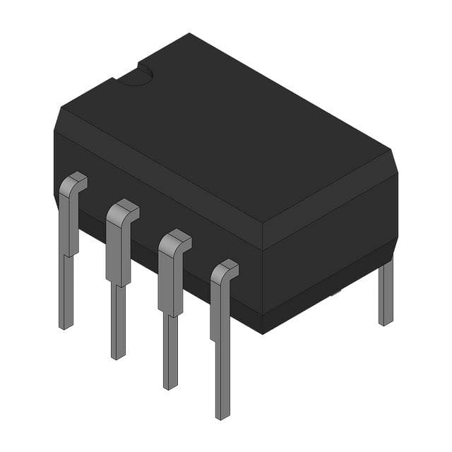
Texas Instruments TLC272CD Overview
The Texas Instruments TLC272CD is a high-precision dual operational amplifier (op-amp) designed for low-power applications, offering both excellent performance and versatility. The device features a CMOS input stage, ensuring a low input bias current, low offset voltage, and high input impedance, making it ideal for sensitive analog signal processing applications. With its wide supply voltage range, rail-to-rail output, and low quiescent current, the TLC272CD is commonly used in a variety of systems, including instrumentation, audio circuits, sensors, and low-power battery-operated devices.
Key Features and Benefits
* Low Power Consumption: The TLC272CD operates with a low quiescent current of only 1.1 mA per amplifier, making it highly suitable for power-sensitive applications, particularly battery-operated systems.
* Rail-to-Rail Output: The device provides rail-to-rail output capability, allowing the output voltage to swing from the negative rail to the positive rail, maximizing the dynamic range and improving performance in low-voltage systems.
* High Precision: Featuring low input offset voltage (typically 50 µV) and low input bias current (typically 1 pA), the TLC272CD offers high accuracy for demanding applications where precise signal amplification is essential.
* Wide Supply Voltage Range: The TLC272CD operates with a wide supply voltage range from 3 V to 36 V (single supply) or ±1.5 V to ±18 V (dual supply), ensuring compatibility with a wide range of system configurations.
* High Slew Rate: With a slew rate of 0.3 V/µs, the TLC272CD provides fast response times, making it suitable for applications requiring quick signal amplification and high-speed operation.
* Low Input Bias Current: With input bias currents typically as low as 1 pA, the TLC272CD is ideal for high-impedance sensor interfacing and precision analog circuitry where minimizing input current is crucial.
* High Common-Mode Rejection Ratio (CMRR): The device features an impressive CMRR of 100 dB, which improves the accuracy of the op-amp in differential signal processing by minimizing errors caused by common-mode signals.
Device Specifications
* Supply Voltage: The TLC272CD is designed to operate with a wide supply voltage range of 3 V to 36 V (single supply) or ±1.5 V to ±18 V (dual supply), making it suitable for various voltage configurations in diverse systems.
* Input Voltage Range: The input voltage range includes 0 V to V+ - 2 V for single-supply operation and ±2 V for dual-supply configurations, ensuring proper operation over a broad range of input conditions.
* Input Offset Voltage: The typical input offset voltage is 50 µV, with a maximum of 500 µV, which contributes to the high accuracy of the device in applications requiring precise voltage amplification.
* Input Bias Current: The device has a low input bias current of 1 pA (typical), which is crucial for high-impedance circuits such as sensors, where minimizing current draw from the signal source is essential.
* Output Swing: The output voltage swing is typically from 0 V to V+ - 0.5 V for a 5 V supply, ensuring full utilization of the supply voltage and making it ideal for low-voltage applications.
* Slew Rate: The TLC272CD has a slew rate of 0.3 V/µs, providing fast response times in applications requiring quick changes in output voltage, such as signal processing and control systems.
* Gain Bandwidth Product: The device offers a gain bandwidth product of 1 MHz, allowing it to maintain high-performance signal amplification across a wide range of frequencies.
* Output Drive Capability: The output drive capability can source or sink up to 20 mA, allowing the device to drive capacitive loads and interface with other components in complex systems.
Package and Pinout
* Package Type: The TLC272CD is available in a DIP-8 (Dual In-line Package) and SOIC-8 (Small Outline Integrated Circuit), making it compatible with both through-hole and surface-mount designs. These packages are compact and reliable, ensuring ease of integration into both prototyping and production systems.
* Pinout: The TLC272CD features a standard 8-pin configuration for both the DIP-8 and SOIC-8 packages. The pinout includes two inverting and two non-inverting inputs, along with the power supply and output pins.
* Pin 1: Offset null (for offset adjustment).
* Pin 2: Inverting input of amplifier A.
* Pin 3: Non-inverting input of amplifier A.
* Pin 4: Ground (for single-supply operation).
* Pin 5: Non-inverting input of amplifier B.
* Pin 6: Inverting input of amplifier B.
* Pin 7: V+ (positive supply voltage).
* Pin 8: Output of amplifier B.
Applications
* Audio Circuits: The low-power and high-precision nature of the TLC272CD makes it ideal for audio amplification, tone control, and filtering in both consumer and professional audio equipment.
* Signal Conditioning: In systems that require amplification of weak signals, such as sensor applications or signal processing systems, the TLC272CD provides a reliable solution with high precision and low offset voltage.
* Instrumentation: The TLC272CD is widely used in instrumentation applications, such as measurement devices, where accurate signal amplification is essential. Its low input bias current makes it suitable for interfacing with high-impedance sensors and transducers.
* Low-Voltage Battery-Powered Systems: Due to its low quiescent current and rail-to-rail output swing, the TLC272CD is ideal for use in battery-powered systems, such as portable sensors, remote monitoring equipment, and low-power embedded applications.
* Active Filters: The device is commonly used in active filter designs, where its low power, precision, and fast response time are essential for maintaining signal integrity and providing accurate frequency filtering.
* Voltage Regulators and Control Systems: The precision of the TLC272CD makes it suitable for use in feedback loops of voltage regulators, where maintaining a stable and accurate output voltage is critical.
Advanced Features
* Offset Adjustment Pin: The TLC272CD includes an offset null pin (Pin 1), allowing users to fine-tune the input offset voltage, improving the accuracy in precision applications where small voltage differences need to be amplified.
* High Common-Mode Rejection Ratio (CMRR): With a typical CMRR of 100 dB, the TLC272CD is highly effective in rejecting common-mode noise, ensuring the integrity of differential signals and preventing interference in sensitive applications.
* Low Drift: The device features a low drift performance, ensuring that the offset voltage and other parameters remain stable over time and temperature fluctuations, contributing to its reliability in long-term applications.
* Wide Temperature Range: The TLC272CD is specified for operation across a temperature range of -40°C to +85°C, ensuring reliable performance in a variety of environments, from industrial to consumer applications.
Conclusion
The Texas Instruments TLC272CD is a versatile, low-power, dual operational amplifier that offers precision, high-speed performance, and reliability for a wide range of applications. With its low offset voltage, rail-to-rail output, and low input bias current, it is an ideal choice for high-precision signal processing in systems such as audio circuits, instrumentation, and low-power systems. The wide supply voltage range, compact package options, and advanced features like offset adjustment and high CMRR make the TLC272CD a powerful tool for engineers looking to enhance performance and efficiency in their analog designs.