Introduction to ON Semiconductor LM358NG
The ON Semiconductor LM358NG is a widely used dual operational amplifier (op-amp) designed for general-purpose applications. It is part of the LM358 family, known for its low power consumption, wide supply voltage range, and ability to operate from a single power supply. The device integrates two independent, high-gain, internally frequency-compensated operational amplifiers in a single package, making it suitable for signal conditioning, filtering, amplification, and other analog processing tasks in various electronic systems.
Device Overview
The LM358NG is particularly valued for its capability to operate at low voltages (starting from 3 V) and its input stage design that allows the input voltage to include ground level, which is advantageous in single-supply operation. This makes it ideal for battery-powered devices and systems where dual power supplies are not available or practical.
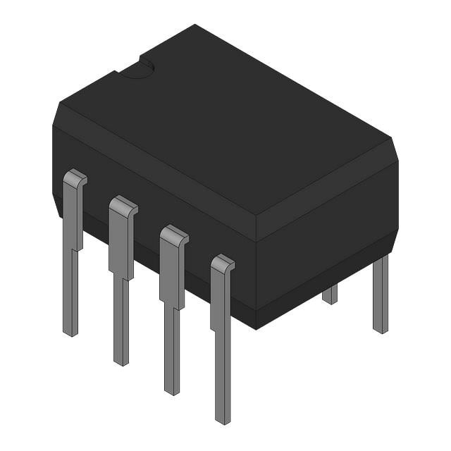
The device is available in several package types; the "NG" suffix typically refers to the SOIC-8 surface-mount package, which offers compactness and ease of PCB integration.
Key Features
- Dual operational amplifiers in one package
- Wide supply voltage range: 3 V to 32 V (single supply) or ±1.5 V to ±16 V (dual supply)
- Low quiescent current: typically 0.5 mA per amplifier
- Input common-mode voltage range includes ground
- Output voltage swing includes ground level, enabling rail-to-rail-like operation on the lower end
- Internally frequency compensated for unity gain stability
- High gain bandwidth product: approximately 1 MHz typical
- Low input offset voltage: typically 2 mV max
- Low input bias current: typically 20 nA
- Wide operating temperature range: -40°C to +85°C (industrial grade)
Electrical Specifications
| Parameter | Conditions | Min | Typ | Max | Unit |
|---------------------------------|----------------------------------|-----------|------------|------------|----------------|
| Supply Voltage (Vcc) | Single supply | 3 | | 32 | V |
| Supply Current per Amplifier | No load | | 0.5 | 0.7 | mA |
| Input Offset Voltage | At 25°C | | 2 | 7 | mV |
| Input Bias Current | At 25°C | | 20 | 250 | nA |
| Input Offset Current | At 25°C | |-20 | +20 | nA |
| Input Common Mode Voltage Range |-0.3 V to (Vcc -1.5 V) typical |-0.3 | | Vcc -1.5 | V |
| Output Voltage Swing | RL=10 kΩ to ground |-0.05 | | Vcc -1.5 | V |
| Gain Bandwidth Product |- | | ~1 | | MHz |
| Slew Rate |- | | 0.3 | | V/μs |
| Total Harmonic Distortion (THD) |- |- |- |- |- |
Pin Configuration
The LM358NG in an SOIC-8 package features:
1. Output A
2. Inverting Input A
3. Non-Inverting Input A
4. Ground (GND)
5. Non-Inverting Input B
6. Inverting Input B
7. Output B
8. Positive Supply Voltage (Vcc)
This pinout enables easy access to both amplifiers with minimal footprint on printed circuit boards.
Functional Description
Each amplifier within the LM358NG consists of a differential input stage followed by gain stages and an output stage optimized for single-supply operation:
- Input Stage: Uses bipolar transistor pairs allowing inputs down to ground level.
- Output Stage: Designed to drive outputs close to ground but not rail-to-rail on the high side; output swing typically extends up to about Vcc minus 1.5 volts.
- Frequency Compensation: Internal compensation ensures stability at unity gain without external components.
These characteristics make the LM358NG suitable for applications requiring accurate signal amplification with low power consumption.
Applications
The versatility of the LM358NG allows it to be used in a broad range of applications including:
- Sensor signal conditioning circuits (e.g., temperature sensors, photodiodes)
- Active filters such as low-pass or high-pass filters
- Integrators and differentiators in analog computation circuits
- Voltage followers/buffers
- Audio preamplifiers and tone controls
- Pulse-width modulation (PWM) circuits and oscillators
- Battery-powered instrumentation due to low supply current and wide voltage range
Operating Conditions
The device performs reliably over industrial temperature ranges (-40°C to +85°C), making it suitable for harsh environments found in automotive electronics, industrial automation, and consumer electronics.
It tolerates supply voltages up to +32 V single-ended or ±16 V dual supplies without damage, providing design flexibility.
Performance Characteristics
The LM358NG’s input offset voltage is relatively low (~2 mV typical), which helps minimize errors in precision measurement circuits but may require calibration or trimming in very sensitive designs.
Its input bias currents are low enough (~20 nA typical) that they do not significantly affect high impedance sources.
The gain bandwidth product of about 1 MHz supports moderate-frequency signals but limits use in very high-speed applications.
Slew rate around 0.3 V/μs indicates moderate speed response suitable for audio frequencies and general analog processing but not for RF or fast transient signals.
Power Consumption
With a quiescent current of approximately 0.5 mA per amplifier at nominal conditions, the LM358NG is considered low-power compared with many older op amps but higher than modern CMOS rail-to-rail devices intended specifically for ultra-low power consumption.
This balance makes it ideal where moderate power efficiency is needed without sacrificing robustness or ease of use.
Reliability and Packaging
ON Semiconductor ensures high manufacturing quality with moisture sensitivity level ratings appropriate for standard PCB assembly processes.
The SOIC package provides good thermal dissipation characteristics while minimizing board space requirements.
Summary of Specifications
| Specification | Value |
|---------------------------------|----------------------------------------|
| Number of Amplifiers | Dual |
| Supply Voltage Range | 3 V – 32 V (single supply) |
| Input Offset Voltage | Max 7 mV |
| Input Bias Current | Max 250 nA |
| Gain Bandwidth Product | ~1 MHz |
| Slew Rate | ~0.3 V/μs |
| Output Voltage Swing |_Down to GND; up to (Vcc –1.5V)_ |
| Operating Temperature Range |-40°C to +85°C |
| Package |_SOIC8_ |
Conclusion
The ON Semiconductor LM358NG remains a popular choice among engineers seeking a reliable, cost-effective dual operational amplifier capable of operating from a single power supply with inputs near ground potential. Its combination of moderate bandwidth, low quiescent current, internal frequency compensation, and wide supply voltage range makes it suitable across numerous analog circuit designs including sensor interfacing, filtering, buffering, and general-purpose amplification tasks in industrial, automotive, consumer electronics, and instrumentation applications.
While not designed for ultra-high-speed or precision instrumentation-grade tasks due to its limited bandwidth and offset specifications, its robust performance under varying conditions ensures continued relevance decades after its introduction into the market.