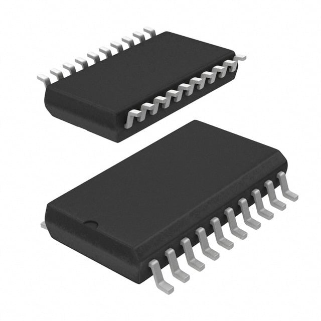
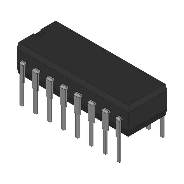
The NXP Semiconductors HEF4044BT,652 is a member of the HEF4000B family of CMOS logic devices and implements a quad R/S latch with complementary outputs. It is designed for general-purpose digital storage and control applications where low static power consumption, wide supply voltage range, and moderate-speed operation are required. The device is fabricated in silicon gate CMOS technology, optimized for compatibility with both CMOS and TTL logic environments while maintaining very low quiescent current consumption.
## Device Function and Logical Architecture
The HEF4044B integrates four independent R/S latch elements within a single package. Each latch provides set (S) and reset (R) inputs, and delivers complementary outputs Q and Q̅. The internal structure is based on cross-coupled NOR latch topology, allowing bistable operation where each latch retains its state indefinitely as long as supply voltage is maintained and no active input transitions occur.
The device is fundamentally an asynchronous storage element. Unlike clocked flip-flops, it does not require a timing reference signal for state changes. Instead, output states are directly controlled by the logic levels applied to the set and reset inputs. This characteristic makes it suitable for control logic, signal conditioning, and simple state retention functions in digital systems.
## Electrical and Supply Characteristics
The HEF4044B belongs to the HEF4000B CMOS logic family, which is characterized by a wide operating supply voltage range. According to the datasheet-defined CMOS logic family behavior, devices in this series typically operate over an extended VDD range suitable for both low-voltage CMOS systems and higher-voltage legacy logic environments. However, the exact guaranteed operating limits, absolute maximum ratings, and recommended operating conditions must be taken strictly from the official NXP datasheet for HEF4044BT,652, as these parameters are tightly specified and not inferred here.
Key electrical characteristics defined at datasheet level include:
* CMOS input structure with very high input impedance
* Extremely low static power dissipation under steady-state conditions
* Rail-to-rail logic input compatibility within supply constraints
* Output drive capability consistent with standard HEF4000B family CMOS outputs
The device exhibits typical CMOS behavior where dynamic power consumption dominates during switching activity, while static power remains negligible.
## Logic Input and Output Behavior
Each latch section responds directly to its corresponding set and reset inputs. The logic truth behavior is defined such that:
* Assertion of set input forces Q output into a defined active state
* Assertion of reset input forces Q output into the complementary state
* Simultaneous inactive inputs maintain previous output state (memory retention)
* Simultaneous activation of both inputs is defined as an indeterminate or forbidden condition in standard R/S latch implementations, with resulting behavior specified in the datasheet truth table
Outputs provide complementary signals, allowing direct use in control logic without additional inversion stages. The output stage is CMOS push-pull, enabling both sourcing and sinking current within the limits specified by the device electrical characteristics.
Propagation delay is present between input transitions and output response, and is defined in the datasheet as a function of supply voltage and load capacitance. These timing parameters are critical for synchronous interfacing but are not required for the internal operation of the latch itself, as it is fundamentally asynchronous.
## Internal Circuit Implementation
The HEF4044B is implemented using CMOS logic gates arranged to form four independent bistable storage cells. Each latch uses a cross-coupled NOR gate configuration, which is a standard implementation for R/S storage elements in CMOS logic families.
The CMOS implementation provides several intrinsic characteristics:
* Near-zero static current consumption due to insulated gate structure
* High noise immunity compared to bipolar logic equivalents
* Symmetrical input threshold behavior relative to supply rails
* Low leakage currents under normal operating conditions
Input protection structures are included to prevent damage from electrostatic discharge and transient voltage conditions, consistent with CMOS device design practices.
## Package and Mechanical Characteristics
The HEF4044BT,652 suffix indicates a specific package and tape/reel or shipping configuration variant. The device is commonly supplied in a standard through-hole or surface-mount plastic package within the HEF4000B family. The exact package type (such as DIP or SO variant), pin pitch, and mechanical dimensions are defined in the manufacturer’s ordering information section and mechanical outline drawing, which are part of the official datasheet documentation.
Pin configuration follows a standardized multi-function mapping:
* Multiple independent R/S latch input pairs
* Complementary output pairs for each latch
* Power supply pins (VDD and VSS)
Pin assignment is fixed and must be followed strictly to ensure correct logic operation.
## Timing and Dynamic Performance Characteristics
The device is not a clocked sequential logic element; however, it exhibits finite propagation delay from input transitions to output response. This delay is dependent on:
* Supply voltage level
* Output load capacitance
* Operating temperature
The datasheet specifies propagation delay values under defined test conditions, typically including capacitive loading and standardized measurement thresholds. These parameters define the maximum switching speed of the device but do not impose a global timing constraint as would be required in synchronous logic systems.
Transition times for output rise and fall edges are also characterized in the datasheet and are influenced by external loading conditions.
## Noise Immunity and CMOS Input Behavior
The HEF4000B CMOS architecture provides defined logic threshold regions with significant noise margins relative to supply voltage. This ensures robust operation in electrically noisy environments and compatibility with mixed-voltage logic systems.
Key characteristics include:
* High input impedance minimizing DC loading effects
* Defined switching thresholds proportional to VDD
* Immunity to slow-rising input signals within specified limits
* Latch-up protection inherent to CMOS process design
These properties make the device suitable for industrial and general-purpose digital control systems where signal integrity may not be ideal.
## Typical Applications
The HEF4044BT,652 is used in digital systems requiring simple memory storage or control state retention without clocked synchronization. Typical applications include:
* Control signal latching in industrial automation systems
* Switch debouncing and state holding circuits
* Simple asynchronous control logic blocks
* Signal conditioning and temporary state storage
* Interface logic in legacy CMOS/TTL mixed systems
Its asynchronous nature makes it particularly suitable for systems where deterministic clocking is not required or where minimal logic overhead is preferred.
## Conclusion
The HEF4044BT,652 is a quad R/S latch CMOS logic device within the NXP HEF4000B family, providing asynchronous bistable storage functionality with complementary outputs. It features CMOS-level low power consumption, wide supply voltage compatibility, and robust input/output behavior suitable for general-purpose digital control applications. Its architecture is based on standard cross-coupled NOR latch structures, and its operational characteristics are defined by datasheet-specified timing, voltage, and load conditions. The device is optimized for simple state storage and control logic integration rather than high-speed synchronous processing or complex sequential logic design.