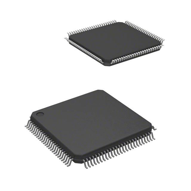
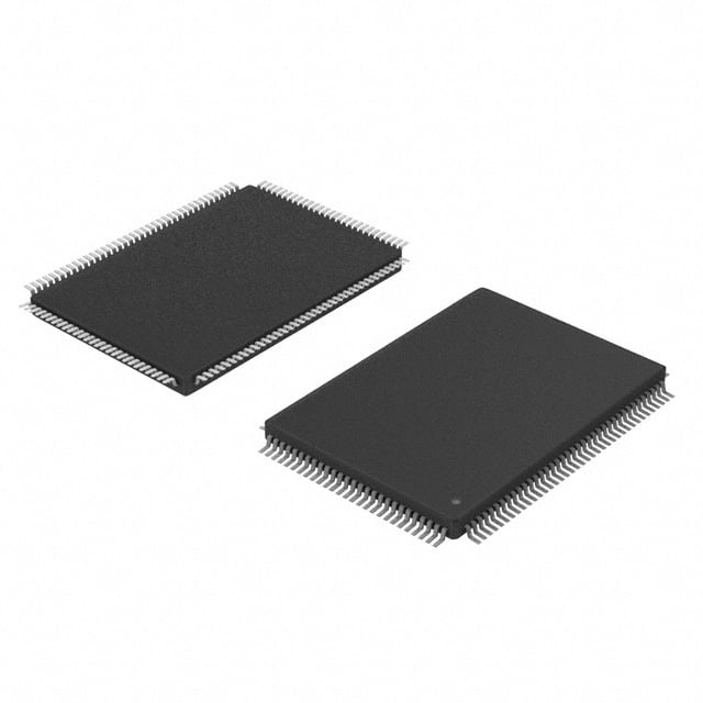
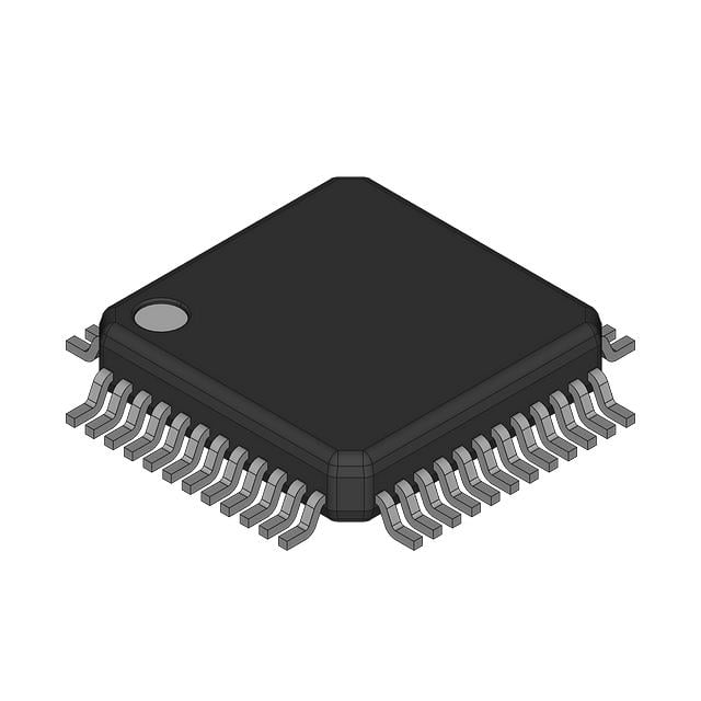
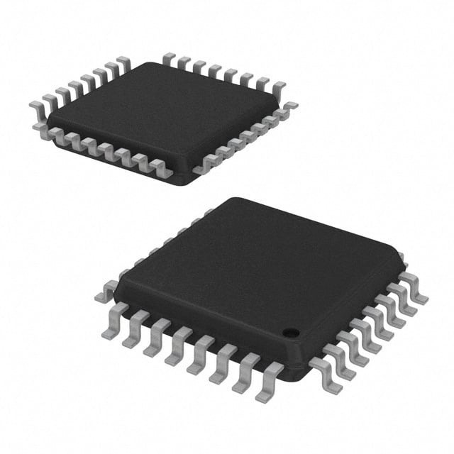
The NXP Semiconductors DSP56F803BU80 is a hybrid digital signal controller belonging to the 56800 core family, integrating a 16-bit digital signal processor (DSP) engine with microcontroller-style peripherals in a single embedded system-on-chip device. It is designed for real-time control applications requiring deterministic signal processing performance combined with embedded control functionality, particularly in motor control, power conversion, and industrial automation systems. The “BU80” suffix identifies the 80 MHz operating frequency grade and specific package configuration within the DSP56F803 product family.
## Core Architecture Overview
The DSP56F803BU80 is built around the 56F800E core architecture, which combines features of a DSP pipeline with a microcontroller instruction set. This hybrid architecture enables efficient execution of both signal processing algorithms and control-oriented firmware within a unified programming model.
The core is based on a modified Harvard architecture, allowing simultaneous access to program and data memory. This enables parallel instruction fetch and data operations, improving throughput for deterministic real-time workloads. The instruction set is optimized for multiply-accumulate (MAC) operations, which are fundamental to DSP algorithms such as filtering, control loops, and modulation.
The device supports both fixed-point arithmetic operations and bit-manipulation instructions, allowing efficient implementation of control algorithms without requiring external DSP co-processors.
## Processing Performance and Execution Model
The DSP56F803BU80 operates at a maximum core frequency of 80 MHz, providing deterministic instruction execution timing. The architecture is designed for single-cycle MAC operations, enabling high computational efficiency for real-time signal processing tasks.
The execution pipeline supports overlapping instruction fetch, decode, and execution stages, which reduces idle cycles and improves instruction throughput. The deterministic timing model is particularly important in control systems such as motor drives, where predictable loop timing is required.
Interrupt handling is designed for low latency, with prioritized interrupt vectors allowing rapid response to external events such as ADC triggers, timer events, or fault conditions.
## Memory Architecture
The memory subsystem of the DSP56F803BU80 consists of integrated program memory and data memory configured in a Harvard-style architecture. This separation allows concurrent access paths for instructions and data, eliminating bus contention during execution.
The device includes on-chip flash memory for program storage and SRAM for runtime data operations. Flash memory is used for non-volatile firmware storage, while SRAM supports stack operations, variable storage, and real-time computational buffers.
The memory architecture is designed to support zero-wait-state operation at the rated core frequency under optimal conditions, enabling predictable execution timing for control loops.
## Peripheral Subsystem Integration
The DSP56F803BU80 integrates a comprehensive set of peripherals designed for embedded control applications. These include analog and digital interface modules tightly coupled to the core processor.
The analog subsystem includes:
* Multi-channel analog-to-digital converter (ADC) for sensor signal acquisition
* Analog comparator modules for threshold detection and protection logic
The digital subsystem includes:
* General-purpose input/output (GPIO) ports
* Timer modules for waveform generation and capture
* Pulse-width modulation (PWM) units for motor and power control applications
* Communication interfaces such as UART, SPI, and I²C for system integration
These peripherals are mapped into the system memory space, enabling register-level control via software instructions.
## PWM and Motor Control Capability
A key functional focus of the DSP56F803BU80 is motor control and power electronics applications. The integrated PWM modules are designed for high-resolution switching signal generation, suitable for controlling power semiconductor devices such as MOSFETs and IGBTs.
The PWM subsystem supports complementary output generation and dead-time insertion, which are critical for preventing shoot-through in half-bridge and full-bridge inverter topologies. The timing resolution of PWM channels allows precise control of duty cycles, enabling advanced control techniques such as field-oriented control (FOC) and sensorless motor control algorithms.
The PWM outputs are tightly synchronized with timer modules and ADC triggering mechanisms, allowing closed-loop control systems with deterministic sampling behavior.
## Analog-to-Digital Conversion System
The integrated ADC subsystem provides multi-channel analog signal acquisition capability for feedback control systems. It is designed to sample external analog signals such as current sensors, voltage dividers, and temperature sensors.
The ADC is typically configured in synchronized mode with PWM or timer events, allowing sampling at precise points in switching cycles. This synchronization is essential in power electronics applications where switching noise must be minimized in measurement signals.
The conversion results are stored in dedicated registers accessible by the DSP core for real-time processing.
## Communication Interfaces
The DSP56F803BU80 includes standard embedded communication peripherals enabling integration into industrial and automotive systems. These interfaces typically include UART for asynchronous serial communication, SPI for high-speed synchronous data transfer, and I²C for low-speed peripheral control.
These communication modules support interrupt-driven operation, reducing CPU overhead during data transmission and reception. This allows the core to focus on real-time control tasks while peripheral data movement occurs autonomously.
## Interrupt and Event Management
The interrupt controller in the DSP56F803BU80 is designed for deterministic real-time response. Multiple interrupt sources from peripherals, timers, and external pins are prioritized through a structured vector table.
The architecture supports nested interrupt handling with programmable priority levels, enabling critical control loops to preempt lower-priority tasks. This is essential in applications such as motor protection, where fault conditions must be handled immediately.
Event-driven execution allows tight coupling between hardware peripherals and software control routines, reducing latency between signal acquisition and control response.
## Power Management and Operating Characteristics
The DSP56F803BU80 is designed for embedded industrial operation with controlled power consumption characteristics. Power usage scales with clock frequency and peripheral activity, with idle modes available to reduce consumption during low-load conditions.
The device supports multiple power modes, including active execution mode and reduced-power standby states. Transition between power modes is controlled via software, enabling dynamic energy optimization in battery-powered or energy-sensitive applications.
Proper decoupling and PCB design are required to ensure stable operation at high switching activity levels, particularly in PWM-heavy control applications.
## System Integration and Application Domains
The DSP56F803BU80 is primarily targeted at embedded control systems requiring deterministic real-time performance. Typical application domains include:
* Brushless DC (BLDC) motor control systems
* AC induction motor drives
* Power inverter and UPS systems
* Industrial automation controllers
* Digital power supply control systems
Its architecture is optimized for closed-loop control systems where analog signal acquisition, real-time computation, and PWM output generation must operate in a tightly synchronized manner.
## Package and Hardware Implementation
The “BU80” suffix identifies a specific package and speed-grade configuration designed for embedded system integration. The device is typically housed in a surface-mount or through-hole package variant suitable for industrial PCB assembly.
Package design considerations include thermal dissipation, pin multiplexing density, and signal integrity for mixed-signal operation. The physical layout supports separation of analog and digital ground domains to minimize noise coupling between subsystems.
## Summary
The NXP DSP56F803BU80 is a 16-bit digital signal controller combining a DSP-oriented execution core with microcontroller peripherals in a unified embedded architecture operating at up to 80 MHz. It integrates flash memory, SRAM, ADC, PWM, timers, and communication interfaces to support real-time control applications. Its hybrid architecture enables deterministic signal processing and embedded control functionality in industrial systems such as motor drives, power conversion systems, and automation controllers, making it a compact and integrated solution for real-time embedded DSP control applications.