Comprehensive Technical Overview of Maxim Integrated 71M6521BE-IGTR/F
The Maxim Integrated 71M6521BE-IGTR/F is a highly integrated digital phase-locked loop (PLL) frequency synthesizer designed primarily for radio frequency (RF) applications, including wireless communication systems, base stations, and instrumentation. This device is recognized for its precise frequency synthesis capabilities, low phase noise, and flexible programmable architecture.
---
General Description
The 71M6521BE-IGTR/F combines a high-performance PLL with an integrated voltage-controlled oscillator (VCO), prescalers, programmable dividers, and an integrated charge pump. This monolithic synthesizer enables the generation of stable, low-noise frequency signals from a single reference input, supporting complex frequency planning and modulation schemes commonly required in RF transceivers and frequency-agile systems.
---
Key Features
* Wide Frequency Range: Typically supports RF output frequencies from approximately 50 MHz up to 1.5 GHz, depending on configuration.
* Integrated VCO: High-quality integrated voltage-controlled oscillator for compact design and stable output.
* Programmable Dividers: Includes programmable integer-N and fractional-N dividers for fine frequency resolution.
* Low Phase Noise: Optimized internal architecture offers superior phase noise performance, critical for RF signal purity.
* Charge Pump & Loop Filter Integration: On-chip charge pump enables tight loop filtering and fast lock times.
* Supply Voltage: Operates typically at 3.3 V supply for core and I/O.
* Low Power Consumption: Efficient design suitable for portable and low-power applications.
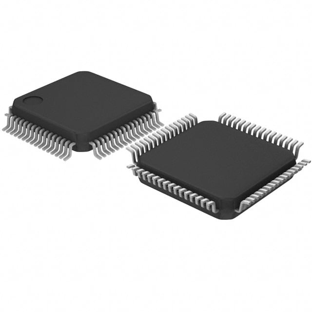
* Package: Available in a compact 32-pin TQFP (Thin Quad Flat Package) suitable for surface mounting.
* Temperature Range: Industrial-grade operation from -40°C to +85°C.
---
Electrical and Performance Specifications
* Operating Supply Voltage (VDD): 3.0 V to 3.6 V
* Reference Input Frequency: Supports input frequencies typically from 10 MHz to 40 MHz (crystal or clock input).
* Output Frequency Range: 50 MHz to 1.5 GHz (dependent on configuration and external components).
* Phase Noise Performance: Typical single-sideband phase noise at 100 kHz offset around -110 dBc/Hz.
* Frequency Resolution: Sub-Hertz frequency tuning resolution via programmable fractional-N synthesis.
* Lock Time: Typically in the order of microseconds to a few milliseconds, depending on loop bandwidth and configuration.
* Spurious Emission: Low spurious signals due to integrated design and loop filter optimization.
* Reference Sensitivity: Supports input reference signals down to approximately 100 mV amplitude.
* Power Consumption: Typically under 50 mW in active operation, varies by output frequency and configuration.
---
Pin and Package Details
* Package Type: 32-pin Thin Quad Flat Package (TQFP), footprint approximately 7 mm x 7 mm.
* Pin Functions: Include power supply, ground, reference input, output signals, programmable control pins for dividers, charge pump outputs, and test interfaces.
* Thermal Characteristics: Junction-to-ambient thermal resistance around 40 °C/W depending on PCB layout.
---
Functional Blocks
* Phase Detector: Compares the divided VCO output with the reference input signal to generate a phase error signal.
* Charge Pump: Converts phase error signal to control voltage for the VCO.
* Voltage-Controlled Oscillator (VCO): Generates frequency output controlled by the charge pump voltage.
* Programmable Dividers: Allow frequency division by selectable integers or fractions to achieve desired output frequency.
* Loop Filter: External passive components used in conjunction with charge pump for loop stability and noise filtering.
---
Applications
* Wireless base stations and repeaters
* RF transceivers and modems
* Test and measurement equipment
* Frequency synthesis for communication protocols (GSM, CDMA, LTE)
* Radar and satellite communication systems
* Clock generation for high-speed digital circuits
---
Design Considerations
* Requires carefully designed external loop filter to balance lock time and phase noise.
* Reference oscillator selection is critical for overall frequency stability and jitter performance.
* PCB layout must ensure low-noise power and ground planes to maintain signal integrity.
* External components like inductors, capacitors, and resistors are required to support PLL loop functionality and VCO tuning.
* Programming interface typically uses serial SPI to set divider values and device modes.
---
Advantages
* High integration reduces overall system component count and board space.
* Programmability provides versatile frequency generation for multi-band systems.
* Low phase noise and spurious emissions ensure superior signal quality.
* Suitable for applications demanding high-frequency stability and rapid frequency hopping.
---
Conclusion
The Maxim Integrated 71M6521BE-IGTR/F is a versatile, high-performance PLL frequency synthesizer ideal for demanding RF and wireless communication applications. Its integrated VCO, flexible divider architecture, and low noise characteristics make it an excellent choice for engineers designing compact, high-quality frequency sources with stringent phase noise and frequency agility requirements. Its robust electrical specifications and industrial-grade packaging further enhance its suitability for a broad range of professional RF system designs.