Let%27s explore the various System-on-Chip (SoC) packaging technologies that have evolved over time. These packaging techniques play a crucial role in connecting and protecting the integrated circuits within an SoC.
1. Traditional Packaging Techniques:
- Wire-Bond Technology:
- Developed in the 1950s, wire-bond technology is still in use today.
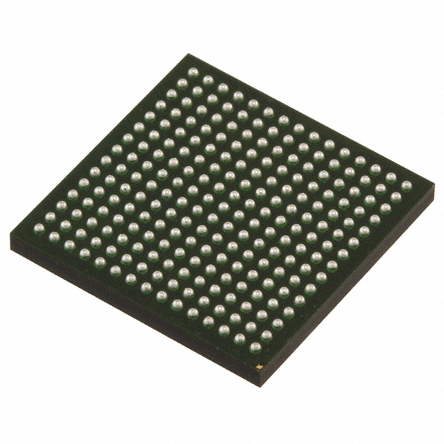
- It involves attaching the printed circuit board (PCB) to the silicon die (the square containing the integrated circuit) using solder balls and thin metal wires.
- While effective, wire-bonding has limitations in terms of performance and density.
2. Advanced Packaging Technologies:
- Over the past two decades, several advanced packaging techniques have emerged to address the limitations of traditional methods:
- 2.5-D Packaging:
- Involves stacking multiple dies (chips) on an interposer (a silicon substrate).
- Interposers provide high-speed connections between the stacked dies.
- This approach enables better performance, reduced power consumption, and improved thermal management.
- 3-D Packaging:
- Similar to 2.5-D, but with additional vertical stacking of dies.
- Stacked dies are interconnected using through-silicon vias (TSVs).
- 3-D packaging offers even higher performance and density.
- Fan-Out Packaging:
- Chips are embedded in a mold compound, and their connections extend beyond the chip boundaries.
- Fan-out packaging provides flexibility in chip placement and routing.
- It is suitable for compact designs and heterogeneous integration.
- System-on-a-Chip (SoC) Packaging:
- Integrates multiple functional blocks (CPU cores, memory, peripherals) into a single chip.
- SoC packaging minimizes external connections and simplifies system design.
- It is commonly used in mobile devices, IoT devices, and automotive applications.
- System-in-a-Package (SiP):
- Combines multiple chips (often different functionalities) within a single package.
- SiP allows heterogeneous integration and modular design.
- It is prevalent in applications where separate chips need to work together (e.g., RF transceivers, sensors, and microcontrollers) ¹².
3. Interposers and Hybrid Bonding:
- For 2.5-D and 3-D packaging, mastering two key technological capabilities is essential:
- Interposers: These silicon substrates provide high-speed connections between stacked dies.
- Hybrid Bonding: A bonding technique that enables precise alignment and electrical connections between stacked dies.
- These technologies enhance the performance and reliability of advanced packaging solutions.
In summary, advanced packaging technologies, such as 2.5-D, 3-D, fan-out, SoC, and SiP, offer innovative ways to overcome the limitations of traditional wire-bonding and flip-chip methods. As demand for high-performance, low-power chips grows, these packaging techniques continue to evolve and shape the semiconductor industry¹².
(1) The growth of advanced semiconductor packaging | McKinsey. https://www.mckinsey.com/industries/semiconductors/our-insights/advanced-chip-packaging-how-manufacturers-can-play-to-win.
(2) The Best 3D Packaging: SoC vs SiP? - Palomar® Technologies. https://www.palomartechnologies.com/blog/bid/73625/The-Best-3D-Packaging-SoC-vs-SiP.
(3) Recent Advances and Trends in Advanced Packaging - IEEE. https://ewh.ieee.org/soc/cpmt/presentations/eps2204c.pdf.
icDirectory United Kingdom | https://www.icdirectory.co.uk/a/blog/what-are-the-different-soc-packaging-technologies.html
☰