Overview
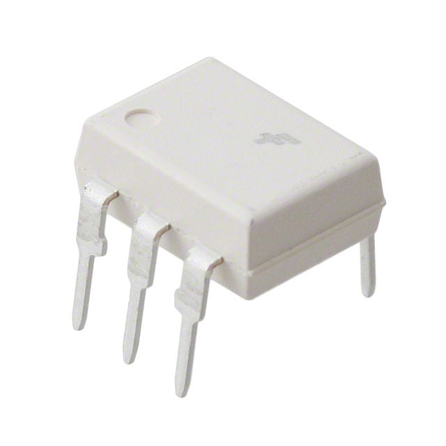
The onsemi H11B3SD is an optocoupler device designed to provide electrical isolation between input and output circuits while enabling signal transmission using optical coupling technology. It integrates a gallium arsenide infrared emitting diode (LED) on the input side and a phototransistor detector on the output side within a compact 4-pin dual in-line package (DIP). This optocoupler is primarily used in switching power supplies, microprocessor system interfaces, and other applications requiring isolation and noise immunity between control and power circuits.
Key Features
* High isolation voltage between input and output for enhanced safety and signal integrity
* High CTR (Current Transfer Ratio) ensuring efficient signal transfer
* Fast response time suitable for switching applications
* Low input current requirement due to efficient LED design
* Compact 4-pin DIP package facilitating easy PCB mounting and integration
* Designed to meet international safety standards for reinforced insulation
Electrical Characteristics
* Input Forward Voltage (V\_F): Typically 1.2 V at 10 mA forward current; maximum forward voltage is around 1.4 V
* Input Forward Current (I\_F): Maximum continuous forward current is 60 mA, with peak forward current up to 1 A for short pulses
* Output Collector-Emitter Voltage (V\_CEO): Maximum voltage rating is 30 V
* Output Collector Current (I\_C): Maximum continuous collector current is 50 mA
* Isolation Voltage (V\_ISO): Rated for 5,000 Vrms (typical) between input and output pins, providing robust isolation for industrial and consumer applications
* Current Transfer Ratio (CTR): Ranges from 50% to 600% depending on input current and operating conditions, typically measured at 10 mA input current and 5 V output voltage
* Collector-Emitter Saturation Voltage (V\_CE(sat)): Low saturation voltage typically less than 0.4 V at I\_C = 2 mA and I\_F = 10 mA, contributing to efficient switching performance
Mechanical and Package Details
* Package: 4-pin Dual Inline Package (DIP)
* Pin Configuration: Pin 1 and 2 are for the input LED (anode and cathode), Pin 3 and 4 for the output phototransistor (collector and emitter)
* Package Dimensions: Standard 6.35 mm pin spacing and overall compact footprint facilitating dense PCB layouts
* Isolation Barrier: Physical separation and internal insulation between input and output to meet safety and regulatory requirements
Performance Parameters
* Response Time: Rise and fall times typically in the range of a few microseconds, enabling usage in moderate-speed digital and analog switching circuits
* Operating Temperature Range: -55°C to +100°C, allowing operation in harsh industrial environments
* Storage Temperature: -55°C to +125°C, ensuring device stability during transportation and storage
* Power Dissipation: Maximum power dissipation on the output transistor side is approximately 150 mW, limiting thermal constraints during continuous operation
Applications
* Isolated switching power supplies: Allows feedback signals to be transmitted across isolation barriers safely
* Microprocessor input/output isolation: Protects low-voltage digital circuits from high voltages and noise
* Signal isolation in industrial controls: Ensures safe signal transfer in noisy or high-voltage environments
* Motor control circuits: Provides isolation between control logic and power electronics
* Telecom and data communication equipment requiring electrical isolation and noise reduction
Reliability and Safety
The H11B3SD meets various safety standards for reinforced insulation, ensuring safe operation in equipment requiring galvanic isolation. Its high isolation voltage and robust packaging contribute to long-term reliability in demanding applications. The device's construction minimizes leakage currents and improves transient immunity, making it suitable for high-voltage isolation tasks.
Typical Usage Considerations
* When designing circuits with the H11B3SD, the input LED current should be carefully controlled to maintain the desired CTR and avoid device damage.
* The output phototransistor should be connected with proper load resistance to optimize switching speed and voltage levels.
* Attention must be paid to PCB layout to maintain isolation creepage distances and prevent accidental shorting or noise coupling.
* Thermal management is essential when operating near maximum power dissipation limits to ensure device longevity.
Summary of Main Specifications
| Parameter | Value |
| ------------------------------------------------- | -------------------------------- |
| Input Forward Voltage (V\_F) | 1.2 V typical @ 10 mA |
| Maximum Forward Current (I\_F) | 60 mA continuous, 1 A peak |
| Output Collector-Emitter Voltage (V\_CEO) | 30 V max |
| Maximum Collector Current (I\_C) | 50 mA |
| Isolation Voltage (V\_ISO) | 5000 Vrms typical |
| Current Transfer Ratio (CTR) | 50% to 600% typical |
| Collector-Emitter Saturation Voltage (V\_CE(sat)) | < 0.4 V at I\_C=2 mA, I\_F=10 mA |
| Operating Temperature Range | -55°C to +100°C |
| Storage Temperature Range | -55°C to +125°C |
| Power Dissipation (Output side) | 150 mW max |
The onsemi H11B3SD optocoupler is a reliable and versatile component well-suited for applications requiring electrical isolation with moderate-speed switching performance and robust safety features. Its combination of high isolation voltage, efficient signal transfer, and industry-standard packaging makes it a popular choice for industrial, consumer, and telecom applications.