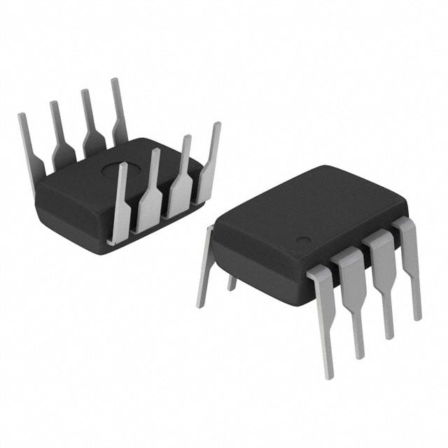
## Product Overview
The onsemi FOD817ASD is a high-performance optocoupler designed for isolating high-voltage circuits from low-voltage control circuitry. It integrates a phototransistor output with an infrared-emitting diode input, providing reliable electrical isolation and signal transfer between circuits operating at significantly different voltage levels. The device is suitable for use in switch-mode power supplies, microcontroller interfacing, motor control circuits, and industrial automation systems requiring galvanic isolation.
## Isolation Characteristics
* Isolation Voltage: 5,300 Vrms between input and output, ensuring protection against high-voltage transients and maintaining safety standards in industrial and consumer applications.
* Creepage and Clearance: Designed for safe operation in printed circuit board layouts, meeting stringent spacing requirements for reinforced isolation.
* Common Mode Rejection: High CMR capability allows operation in noisy environments, reducing susceptibility to interference from switching power circuits.
## Input LED Characteristics
* LED Forward Voltage: Typically 1.25 V at 10 mA forward current, allowing compatibility with standard logic-level drivers.
* Forward Current: Maximum continuous forward current is 60 mA, supporting high drive currents for rapid response.
* Input Current for Saturation: Minimum LED current required to achieve transistor saturation is 10 mA, ensuring predictable operation in switching applications.
* Wavelength: Infrared emission centered at approximately 940 nm, optimized for phototransistor sensitivity and efficiency.
## Output Phototransistor Characteristics
* Collector-Emitter Voltage: Maximum rating of 80 V, enabling direct interface with standard 5 V to 24 V logic and industrial control circuits.
* Collector Current: Maximum continuous collector current of 50 mA, providing sufficient drive capability for downstream circuitry without additional amplification in many applications.
* Current Transfer Ratio (CTR): Typical CTR ranges from 50% to 600% depending on input current and temperature, ensuring flexibility in circuit design.
* Rise and Fall Times: Typical response times of 3 µs rise and 3 µs fall, allowing high-speed switching for PWM and digital signal applications.
## Electrical Performance
* Isolation Capacitance: Approximately 0.8 pF typical, minimizing signal coupling and maintaining high fidelity in fast switching circuits.
* Input-Output Delay: Propagation delay is typically 4 µs, suitable for moderate-speed digital isolation applications.
* Saturation Voltage: Low VCE(sat) of typically 0.3 V at nominal collector current, reducing power dissipation in the output stage.
* Leakage Current: Very low collector-emitter leakage current, typically 10 nA at maximum rated voltage, enhancing safety and preventing false triggering.
## Thermal and Power Specifications
* Operating Temperature Range: –55°C to +100°C, supporting industrial and automotive environments.
* Storage Temperature Range: –55°C to +150°C, ensuring reliable storage and handling.
* Power Dissipation: Maximum total power dissipation is 200 mW at the phototransistor output, requiring adequate PCB thermal design to avoid overheating.
## Package and Mounting
* Package Type: 6-pin DIP (dual in-line package), providing easy through-hole assembly for prototyping and PCB integration.
* Isolation Barrier: Internal construction ensures the input LED and output phototransistor are fully separated by an insulating layer for reinforced isolation.
* Pin Configuration: Standard input/output arrangement with clear identification of anode, cathode, collector, emitter, and optional base connection for transistor biasing or feedback.
* Mounting Considerations: Compatible with automated insertion and soldering processes, with recommendations for lead spacing and PCB creepage to maintain isolation integrity.
## Reliability and Compliance
* Safety Standards: Meets international safety standards for reinforced isolation in industrial and consumer equipment.
* Moisture Sensitivity: Classified according to JEDEC standards, ensuring reliable performance during storage and assembly.
* Long-Term Reliability: Solid-state construction with encapsulated LED and phototransistor ensures long operational life, exceeding 50,000 hours under nominal operating conditions.
## Typical Applications
* Switch-Mode Power Supplies: Provides galvanic isolation between high-voltage input stages and low-voltage control circuitry.
* Microcontroller Interfacing: Protects MCU or digital logic from voltage transients and noise in industrial systems.
* Motor Control: Ensures safe isolation between control logic and high-current motor drive circuits.
* Industrial Automation: Suitable for isolating sensor signals and actuator control circuits in factory automation systems.
* Signal Isolation: Maintains signal integrity in noisy environments while providing safe electrical separation between system domains.
## Summary
The onsemi FOD817ASD optocoupler is a robust and versatile solution for applications requiring electrical isolation with fast response times and high reliability. Its reinforced isolation, low saturation voltage, wide operating temperature range, and high CTR make it suitable for interfacing, switching, and protective functions in industrial, automotive, and consumer electronics. Its standard DIP packaging and low input drive requirements allow flexible integration into a variety of circuit designs, ensuring safety, signal integrity, and efficient operation.