## Texas Instruments CSD18510KTT Overview
The Texas Instruments CSD18510KTT is a dual N-channel MOSFET designed for high-performance power management applications. This device is part of the NexFET™ family, which is known for its advanced technology that offers low on-resistance (R_DS(on)), fast switching speeds, and high efficiency. The CSD18510KTT is ideal for a variety of applications, including DC-DC converters, power supplies, motor drives, and battery management systems.
## Key Features
1. Dual N-Channel Configuration: The CSD18510KTT integrates two independent N-channel MOSFETs in a single package, which helps save PCB space and simplifies design.
2. Low On-Resistance: The device features very low R_DS(on), which minimizes conduction losses and improves overall efficiency in power conversion circuits.
3. High Switching Speed: The MOSFET is designed for fast switching, enabling efficient operation at high frequencies.
4. Thermal Performance: The package has been engineered to provide excellent thermal management, allowing for higher current ratings without overheating.
5. Low Gate Charge (Q_g): The device exhibits low gate charge characteristics, which further enhances switching performance and reduces power loss during operation.
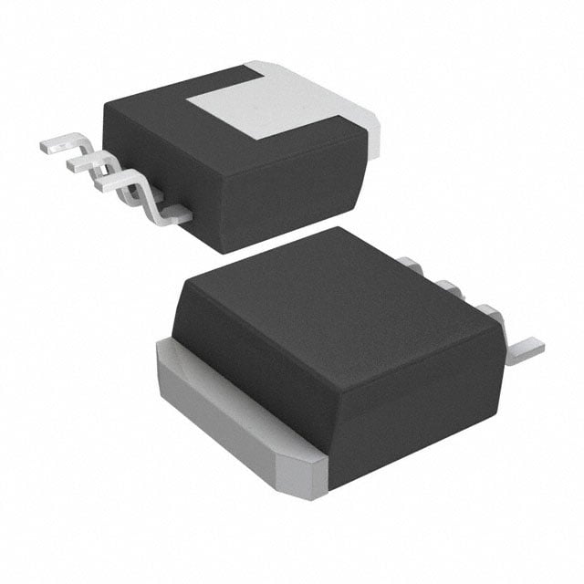
6. Robust Packaging: Housed in a compact 8-pin VQFN package, the CSD18510KTT offers a high level of integration and is easy to mount on printed circuit boards.
7. High Voltage Rating: Suitable for high-voltage applications, it delivers reliable performance under demanding conditions.
## Specifications
Here are the detailed specifications of the CSD18510KTT:
- Device Type: Dual N-Channel MOSFET
- Package Type: VQFN (Very Thin Quad Flat No-lead) – 8 Pins
- Dimensions: 3 mm x 3 mm x 0.75 mm
- Lead Finish: NiPdAu
- Maximum Drain-Source Voltage (V_DS):
- Rated Voltage: 30V
- Continuous Drain Current (I_D):
- At 25°C: 30A per channel
- At 100°C: 20A per channel
- On-Resistance (R_DS(on)):
- At V_GS = 10V: Typically 5.5 mΩ
- At V_GS = 4.5V: Typically 7.0 mΩ
- Gate Charge (Q_g):
- Total Gate Charge: 10 nC (typical at V_GS = 10V)
- Input Capacitance (C_iss):
- Typical: 1400 pF
- Output Capacitance (C_oss):
- Typical: 300 pF
- Reverse Transfer Capacitance (C_rss):
- Typical: 80 pF
- Thermal Resistance:
- Junction-to-Case (RθJC): 1.8 °C/W
- Junction-to-Ambient (RθJA): 40 °C/W (with adequate thermal management measures)
- Operating Temperature Range:
- -55°C to +150°C
## Applications
The CSD18510KTT is suited for a wide range of applications, including:
1. DC-DC Converters: Ideal for use in step-down (buck) converters where efficiency is crucial.
2. Power Supplies: Suitable for both AC-DC and DC-DC power supply designs, enhancing performance and reliability.
3. Battery Management Systems: Used in battery chargers and protection circuits to improve energy efficiency.
4. Motor Drives: Effective in driving applications such as brushless DC motors, enhancing performance with less heat generation.
5. Telecommunications: Can be used in power amplifiers and other RF applications due to its high-frequency capabilities.
6. Consumer Electronics: Incorporated into devices requiring efficient power conversion and management.
## Conclusion
The Texas Instruments CSD18510KTT stands out as a highly efficient dual N-channel MOSFET that offers low on-resistance, high-speed switching, and robust thermal performance. Its compact packaging and superior electrical characteristics make it an excellent choice for a variety of power management applications. Whether designing for consumer electronics, automotive, or industrial equipment, the CSD18510KTT provides the necessary performance and reliability to meet modern demands.