Introduction
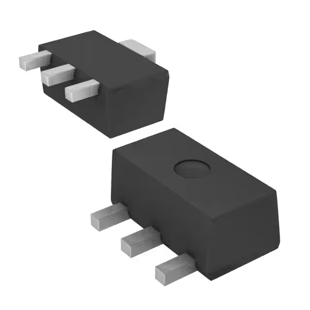
The 2DB1714-13 is a low VCE(sat) PNP surface mount transistor from Diodes Incorporated. It features epitaxial planar die construction and is designed specifically for medium power switching and amplification applications. The device provides a high continuous collector current rating of 2 A combined with exceptionally low collector-emitter saturation voltage, making it suitable for efficient power management in compact designs. Packaged in the SOT89-3L outline with the -13 suffix indicating tape-and-reel packaging of 2500 units, this transistor is the PNP complement to the 2DD2679 NPN device. It is fully RoHS compliant, lead-free by design, and classified as a "Green" device with UL 94V-0 flammability rating. Note that the part is listed as obsolete and discontinued in the manufacturer's documentation.
Key Features
The 2DB1714-13 delivers optimized performance through its low saturation voltage and robust current handling. It supports a collector-emitter breakdown voltage of 30 V and emitter-base breakdown of 6 V. The DC current gain ranges from 270 to 680 under specified test conditions. Peak pulse current reaches 4 A while maintaining continuous operation up to 2 A. The device offers a typical transition frequency of 200 MHz and low output capacitance of 16 pF. Additional advantages include suitability for automated assembly processes, matte tin lead finish for reliable soldering, and moisture sensitivity level 1 per J-STD-020. These characteristics enable efficient switching with minimal power loss in medium-current applications.
Typical Applications
This PNP transistor is widely used in medium power switching circuits such as DC-DC converters, motor drivers, relay drivers, and load switches. It also performs well in linear amplification stages, audio output stages, and voltage regulation circuits where low VCE(sat) improves efficiency and reduces heat generation. Common deployments include consumer electronics power management, industrial control interfaces, battery-powered equipment, and automotive auxiliary systems requiring compact surface-mount solutions with high current capability.
Device Construction
The 2DB1714-13 utilizes epitaxial planar technology with a PNP structure on a silicon die. The collector, base, and emitter regions are formed through precise diffusion and epitaxial growth processes to achieve low on-state resistance and high breakdown voltages. Internal die construction ensures uniform current distribution and minimizes parasitic effects. The device is assembled in a plastic molded SOT89-3L package with a copper leadframe for excellent thermal and electrical performance.
Absolute Maximum Ratings
All ratings are specified at an ambient temperature of 25 °C unless otherwise noted. Collector-base voltage is rated at 30 V, collector-emitter voltage at 30 V, and emitter-base voltage at 6 V. Continuous collector current is 2 A with a peak pulse current of 4 A. Power dissipation reaches 0.9 W on minimum recommended pad layout or 2 W on 1 inch² copper pad layout. Operating and storage junction temperature range extends from 55 °C to +150 °C. These limits must not be exceeded to prevent permanent damage to the device.
Thermal Characteristics
Power dissipation is 0.9 W when mounted on an FR-4 PCB with the minimum recommended pad layout, corresponding to a junction-to-ambient thermal resistance of 139 °C/W. With an expanded 1 inch² copper pad layout on FR-4, power dissipation increases to 2 W and thermal resistance drops to 62.5 °C/W. These values allow reliable operation in surface-mount assemblies when proper heat sinking and airflow are provided. The device is rated for full performance across the industrial temperature range.
Electrical Characteristics
DC electrical parameters are measured at 25 °C under pulsed conditions where noted. Collector-base breakdown voltage is at least 30 V at 10 µA collector current. Collector-emitter breakdown voltage is 30 V at 1 mA collector current. Emitter-base breakdown is 6 V at 10 µA emitter current. Collector and emitter cutoff currents remain below 0.1 µA at rated reverse voltages. In the on state, collector-emitter saturation voltage is maximum 370 mV at 1.5 A collector current and 75 mA base current. DC current gain measures between 270 and 680 at 2 V collector-emitter voltage and 200 mA collector current.
Small Signal Characteristics
Small-signal performance includes an output capacitance of 16 pF typical measured at 10 V collector-base voltage and 1 MHz. The current gain-bandwidth product is typically 200 MHz at 2 V collector-emitter and 100 mA collector current. These parameters support operation in switching and amplification circuits up to several hundred megahertz while maintaining low distortion and fast response.
Pin Configuration and Package Outline
The SOT89-3L package houses the transistor with standard three-lead configuration: the center tab serves as the collector connection while the outer leads provide base and emitter access in the conventional SOT89 orientation for PNP devices. Body dimensions include length from 4.40 mm to 4.60 mm, width from 2.40 mm to 2.60 mm, and height from 1.40 mm to 1.60 mm. Lead width is 0.45 mm to 0.55 mm with specific forming for surface mounting. The package weight is approximately 0.072 grams and features matte tin plating over copper leadframe.
Ordering and Marking Information
The complete ordering code 2DB1714-13 specifies the SOT89-3L package supplied in 2500-unit tape-and-reel format. The marking code on the package top consists of “1714” followed by the date code “YWW”, where Y represents the last digit of the year and WW the week number. This marking enables traceability and identification during assembly and inspection processes. The device was offered in standard commercial temperature grade and is no longer in active production.
Suggested Pad Layout and Assembly Notes
Recommended PCB pad dimensions support reliable solder joints and thermal performance: specific X and Y coordinates provide adequate copper area for heat spreading. The device is compatible with standard reflow soldering profiles and automated pick-and-place equipment. Proper attention to thermal design is required to stay within dissipation limits during continuous high-current operation.